Biren BR100: China with extremely powerful GPU in 7nm process

Birentech has introduced an all-purpose GPU that is said to beat Nvidia’s A100 in terms of its raw computing power and is manufactured in the 7 nm process. The graphics card is equipped with 64 GiB of HBM2e memory and is only available in the OAM form factor. Only Nvidia’s H100 should clearly beat the Chinese graphics card. Read more about this below.
Own production and development of semiconductor elements provides a certain security, especially in times of shortages and crises, and now that Russia has started to construct “own” chips and laptops (we reported), it is no wonder that China has already taken several steps is further and has presented a very powerful GPU for AI calculations that should clearly beat Nvidia’s Ampere-based A100. The GPU was manufactured by Birentech, a small company from Shanghai.
Five years of Radeon Vega: The last GCN generation with up to 16 GiByte HBM [Update: RX Vega wird fünf]
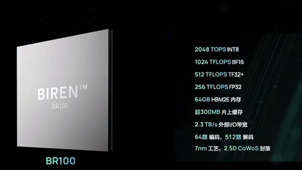
The Biren BR100 itself has nothing to do with small. The GPU is manufactured using the current 7nm process and contains 77 billion transistors, just three billion fewer than Nvidia’s hopper-based H100. It is manufactured in the TSMC 1.5D CoWoS design and includes 300 MiB cache, 64 GiB HBM2e memory with a memory bandwidth of 2.3 Tb/s and native support for PCI-E 5.0.
Birentech BR100
Source: Wccftech
In the presentation, the manufacturer addressed the performance of the new flagship. The BR100 should achieve 2,048 TOPs (INT8), 1,024 TFLOPs (BF16), 512 TFLOPs (TF32+) and 256 TFLOPs (FP32). According to the manufacturer, Nvidia’s A100 achieves 624 or 1,248 TOPS (INT8), 312 or 624 TFLOPs (BF16), 156 or 312 TFLOPs (TF32) and 19.5 TFLOPs (FP32). The extent to which these metrics are true cannot yet be verified, but if they are correct, Nvidia’s A100 is beaten and only the H100 delivers 2 to 2.5 times the performance of the Chinese GPU.
Compared to the H100, however, the small difference in transistors must mean that the GPU is huge and correspondingly expensive to manufacture. The H100 already measures 814mm², but is manufactured in TSMC’s 4nm process and not in 7nm. Birentech specifies the TDP as 550 watts and the graphics card will only be offered as an OAM module, while a reduced expansion stage as a PCI-E model with a TDP of 300 watts will soon follow.
Source: Wccftech
Reference-www.pcgameshardware.de