AMD Radeon RX 7900 XTX and RX 7900 XT in the test: “double boom” against Nvidia’s Geforce RTX 4080
2022 will go down in hardware history as a special year, that’s for sure with the start of the Radeon RX 7000 generation at the latest. The density of new releases, especially when it comes to graphics cards, and the associated price controversies are unbeatably high. Now the brilliant finale is imminent: AMD is sending the RDNA 3 architecture announced on November 3rd into the race for the favor of PC enthusiasts and would like to offer powerful but significantly cheaper alternatives to Nvidia’s Geforce RTX 4080. The official prices for the Radeon RX 7900 XTX and Radeon RX 7900 XT are 1,149 or 1,049.99 euros (RRP) and seem almost too good to be true. PCGH clarifies whether there is a catch in the big test of the AMD Radeon RX 7900 XT and XTX.
Radeon RX 7900 XT(X) review: position and specification
You read that correctly, with the new top model Radeon RX 7900 XTX AMD is not aiming at the Geforce spearhead RTX 4090, but a little lower – the Geforce RTX 4080 is the declared goal. As we know since testing the RTX 4080, this is not an easy task, because the second largest graphics card based on the Ada Lovelace architecture is fast, efficient and quiet. However, the Geforce RTX 4080 also has some shining weak points in its otherwise flawless armor: It offers “only” 16 GiByte memory, no Displayport 2.1, relies on a controversial new power socket, requires a lot of space in the case, renders significantly slower than the RTX 4090 and is still very expensive. If you nod to one or all of the above points, you belong to the target group for a Radeon RX 7900 XTX or Radeon RX 7900 XT. But first things first.
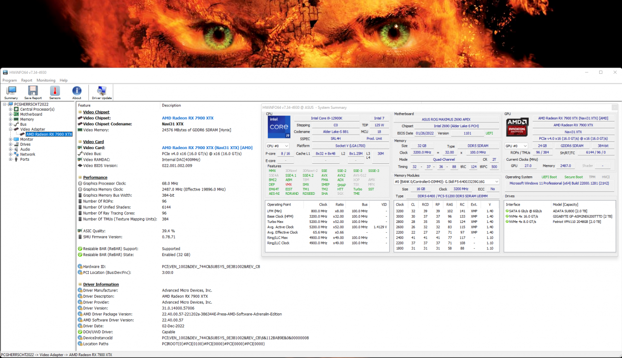
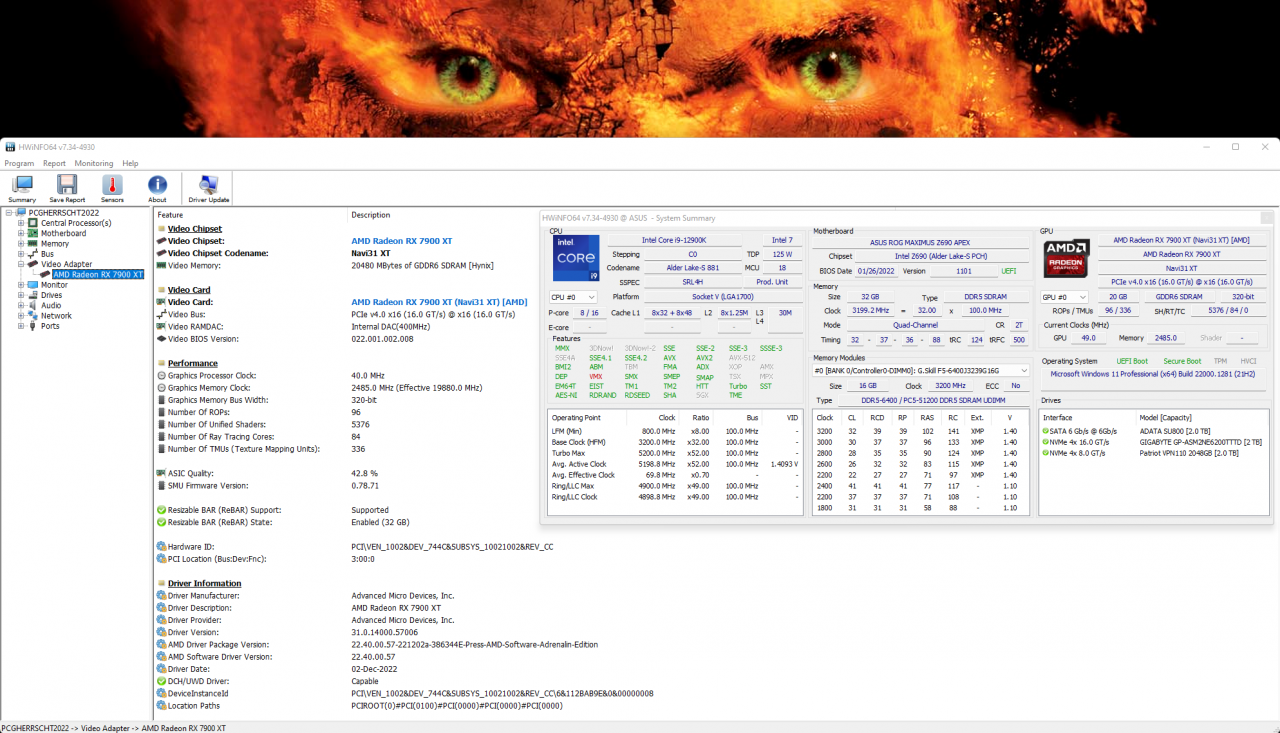
Radeon RX 7900 XTX & XT: Hwinfo Overview
Also worth reading: Buy the RX 7900 XT(X): Here the chances of a cheap RTX 4080 killer are greatest
As physical limitations make it increasingly difficult to produce faster graphics chips without prohibitive costs, engineers around the world are tinkering with ideas to circumvent the unsolvable problem. With RDNA 3, the third iteration of AMD’s GPU microarchitecture released in 2019, the Canadians aren’t bluntly targeting the performance crown, but also manufacturing costs. The latter are partly responsible for the price misery, which Navi 31 is the first GPU based on chiplets.
Nvidia broke the fence with the Geforce RTX 4090 and RTX 4080. Only one manufacturer has the expertise and facilities to produce state-of-the-art graphics processors: the Taiwanese foundry TSMC, which has its services gold-plated. With RDNA 3, AMD is therefore porting the experience of its processor teams to the world of graphics chips – Navi 31 is the first GPU based on chiplets. Instead of a monolithic mega chip à la Nvidia, AMD is swapping out parts for maximum yield in the form of multiple small chips with custom manufacturing. In the case of the Radeon RX 7900 XT and XTX as chiplet pioneers, this means: A so-called graphics compute die (GCD) is combined on a substrate with six memory cache dies (MCD) and together forms the Navi 31 unit. If you want to know more , which advantages and disadvantages this procedure has, click on to the next page, which deals with RDNA 3 in general and Navi 31 in particular.
If you compare Navi 31 with its predecessor Navi 21, it becomes clear that AMD is not going to the limit: The number of FP32 ALUs increases by only 20 percent, while the memory subsystem increases by 50 percent – the level 3 cache exempt. The latter, referred to by AMD as the second generation Infinity Cache, is no longer in the core (as with RDNA 2), but in the six external MCDs, each with 16 MiByte. According to AMD, the resulting 96 MiByte L3 cache in the Navi 31 is no disadvantage compared to the Navi 21 thanks to the improved hit rate and larger L0 to L2 caches Keeping data at its core is the way to go. Because everything that has to be requested in the graphics memory takes a relatively long time and also costs a lot of energy. Not only in retrospect does RDNA 2 prove to be a signpost – Nvidia now also relies on huge caches to drastically increase (energy) efficiency. The difference to RDNA 3 lies in the detail – more on the next page. Let’s first take a look at all performance-related parameters of the Radeon RX 7900 XT and RX 7900 XTX in comparison with other (ex) high-end graphics cards:
| graphic card | RX 7900 XTX | RX 7900 XT | RX 6950 XT | RTX 4090 | RTX 4080 |
|---|---|---|---|---|---|
| market launch | 13.12.2022 | 13.12.2022 | 05/10/2022 | 10/12/2022 | 11/16/2022 |
| architecture | RNA 3 | RNA 3 | RDNA 2 | Ada Lovelace | Ada Lovelace |
| Codename/Confection | Navi 31 XTX | Navi 31 XT | Navi 21 KXTX | AD102-300 | AD103-300 |
| Chip Size (Die/GCD) | 300mm² | 300mm² | 520mm² | 608.5mm² | 378.6mm² |
| Size Memory Cache Dies (MCD) | 6× ~37 = 220mm² | 6× ~37 = 220mm² | – | – | – |
| Transistors graphics chip (bn.) | 57.7 (including MCDs) | 57.7 (including MCDs) | 26.8 | 76.3 | 45.9 |
| manufacturing process | N5 (GCD) + N6 (MCD) | N5 (GCD) + N6 (MCD) | N7 | 4N | 4N |
| Shader Clusters (CUs/SMs) | 96 | 84 | 80 | 128 | 76 |
| FP32 ALUs/TMUs/ROPs | 6,144*/384/192 | 5,376*/336/192 | 5.120/320/128 | 16.384/512/176 | 9.728/304/112 |
| Ray Tracing Units | 96 (2nd gen.) | 84 (2nd gen.) | 80 (1st gen) | 128 (3rd Gen.) | 76 (3rd Gen.) |
| Matrix Units | 192 (1st Gen.) | 168 (1st Gen.) | – | 512 (4th Gen.) | 304 (4th gen.) |
| Level 2 cache (MiB) | 6 | 6 | 4 | 72 | 64 |
| Level 3 cache (MiB) | 96 | 80 | 128 | – | – |
| GPU Boost Clock in Games (MHz) | 2,300** | 2,000** | 2,100 | 2,520 | 2,505 |
| FP16 Performance ALUs (TFLOPS) | 113 | 86 | 46.1 | 82.6 | 48.7 |
| FP32 Performance ALUs (TFLOPS) | 56.5 | 43 | 21.5 | 82.6 | 48.7/0.76 |
| Fill rate (Mtex/Mpix per sec) | 883.2/294.4 | 672.0/256.0 | 672.0/268.8 | 1,290.2/443.5 | 761.5/280.6 |
| Optical Frame Accelerator (TOPS) | – | – | – | ~305 | ~305 |
| Memory Binding (Bit) | 384 | 320 | 256 | 384 | 256 |
| L3 cache speed (MHz) | 2,300 | 2,300 (probably) | 1,940 | – | – |
| Speed RAM (GTs/MHz) | 20.0/10,000 | 20.0/10,000 | 18.0/9,000 | 21.0/10,502 | 22.4/11,200 |
| storage type | GDDR6 | GDDR6 | GDDR6 | GDDR6X | GDDR6X |
| Transfer rate memory (GB/s) | 960 | 800 | 576 | 1,008 | 717 |
| L3 cache transfer rate (TB/s) | 5.3 | 5.3 (presumably) | 2 | – | – |
| Storage capacity (MiB) | 24,576 | 20,480 | 16,384 | 24,576 | 16,384 |
| PCI Express standard | 4.0×16 | 4.0×16 | 4.0×16 | 4.0×16 | 4.0×16 |
| PCI Express power connectors | 2× 8 pin | 2× 8 pin | 2× 8 pin | 1× 16-/4× 8-pin | 1× 16-/3× 8-pin |
| Power consumption (board power) | 355 watts | 315 watts | 335 watts | 450 watts | 320 watts |
| (Display) connectivity | DP 2.1, HDMI 2.1a, USB-C | DP 2.1, HDMI 2.1a, USB-C | DP1.4a, HDMI2.1a | DP1.4a, HDMI2.1a | DP1.4a, HDMI2.1a |
| Recommended price (USD) | 999 | 899 | 1,099 | 1,599 | 1,199 |
| Recommended price (euros) | 1.149 | 1,049.99 | 1,239 | 1,859 | 1,399 |
Specifications of the performance with typical GPU boost according to the manufacturer. Data verified by own tests and inquiry at AMD/Nvidia. In practice, the frequency varies (usually it is higher) and therefore the throughput. *ALUs with new “Dual Issue” skill, which at best (!) behave like double the number. **Specified is the “Game Clock”; Navi 3x introduces another clock domain for the front end, which works faster (2,500 MHz on the XTX).
In addition to higher clock rates for the GPU and memory, RDNA 3 offers another trick to get the most out of the limited space: the revised RDNA 3 compute units are able to achieve twice the throughput for FP32 calculations. If you are now thinking of Nvidia’s Ampere (Geforce RTX 30), you are on the right track. Although the implementation is different, the problems are similar: In contrast to fully doubled arithmetic units including all registers and other details, a transistor-saving doubling does not always work. AMD therefore does not speak of 12,228/10,752, but officially of 6,144/5,376 FP32 ALUs for the Radeon RX 7900 XTX/XT. The specified arithmetic peak values (“up to”) are correct and also legally safe, but current gaming practice teaches that a Radeon RX 7900 XT does not even remotely achieve a factor of 2 compared to a RX 6950 XT, even if it is officially 43 instead of 21 TFLOPS. A good keyword for the benchmarks – the next page, however, is initially devoted to further architecture details.
Reference-www.pcgameshardware.de